
Wafer Aligner
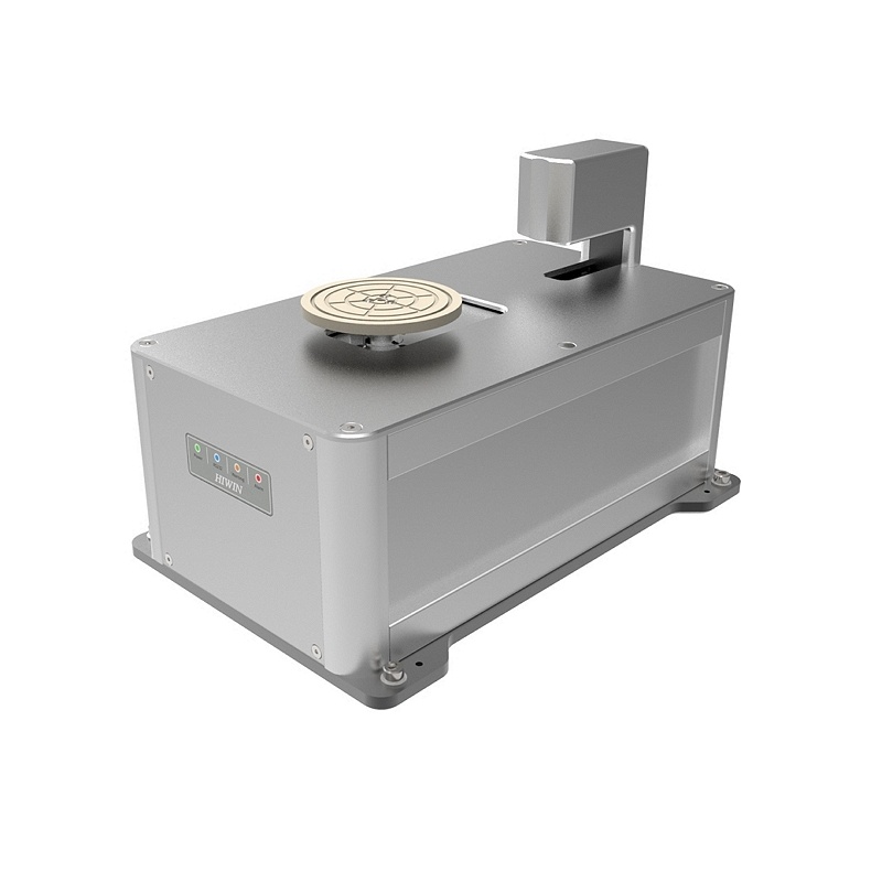
Key Features
Industry's smallest footprint; supports detection of various materials and contours; completes wafer edge finding, center and angle correction in as little as 4.9 seconds.
Center Repeatability
±0.1
Notch Angle Repeatability
±0.2°
Edge Finding Time
<5.9
Applications
HIWIN Technical Support
Semiconductor Subsystems · Wafer Aligner
Technical Description and Selection ReferenceProduct Overview
The wafer aligner is part of HIWIN Technologies' (HIWIN) semiconductor subsystem product line. With the industry's smallest footprint, it supports detection of various materials and contours and completes wafer edge finding, center and angle correction in as little as 4.9 seconds.
Product Features
- Industry's smallest footprint; supports detection of various materials and contours; completes wafer edge finding, center and angle correction in as little as 4.9 seconds.
Center Repeatability
±0.1
Notch Angle Repeatability
±0.2°
Edge Finding Time
<5.9
Applications
The wafer aligner is widely used in the semiconductor industry and other applications, meeting the requirements for stability and precision in precision transmission, automated production and industrial upgrading.
About HIWIN Technologies
HIWIN Technologies (HIWIN) is a leading global manufacturer of motion control products and system technologies, specializing in the R&D and manufacturing of precision ball screws, ball splines, linear guideways, single-axis and multi-axis robots, harmonic drives, torque motors and other products, providing high-precision, high-rigidity motion solutions for industries such as semiconductors, flat panel displays, machine tools, automation equipment and industrial machinery.
 Previous
Already the first article
Previous
Already the first article
 Next
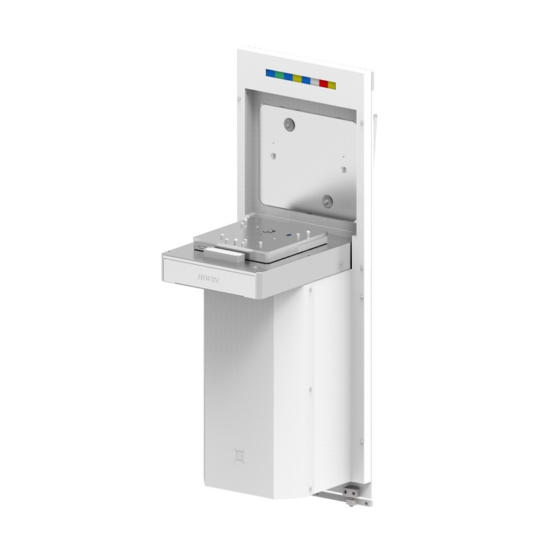
Wafer Loader / Load Port
Next
Wafer Loader / Load Port
Frequently Asked Questions
We provide Semiconductor Subsystems for semiconductor manufacturing — wafer transfer systems, wafer robots, wafer loaders and precision positioning stages designed for cleanroom environments, delivering the reliability required for 24/7 production.
Yes. The Wafer Aligner is designed and manufactured for cleanroom use, with sealed bearings, low particle generation and vacuum-compatible options where required.
Our wafer transfer systems handle standard wafer sizes with high throughput and precise alignment. Send us your wafer size, cycle time and cleanroom class for a specification.
Yes. We supply Semiconductor Subsystems as complete solutions including robots, loaders, alignment stages, controllers and software, integrated and tested before delivery.
Our Semiconductor Subsystems are engineered for semiconductor-grade reliability with long-life components and rigorous testing, minimizing downtime in demanding production environments.
Please send your application requirements — wafer size, throughput, cleanroom class and interface needs — and we will reply with a technical proposal and quotation within 24 hours.
Buying Semiconductor Subsystems from China
is Your Best Choice!
Genuine quality at factory-direct prices — we ship worldwide, support non-standard customization, and offer volume discounts for bulk purchases. Get your quotation within 24 hours.